
The tech world is buzzing after a major declaration, Synopsys and Samsung jointly revealed a deep collaboration on AI-powered Electronic Design Automation (EDA) tools for next-generation 2nm and 3nm processes. The partnership, announced at the Samsung SAFE Forum 2026, promises production-ready design flows that could dramatically accelerate the development of complex AI chips. While the press release paints a picture of seamless innovation, our analysis reveals a far more complex and challenging road ahead for ai-powered eda. This development isn’t just about faster chips; it’s a high-stakes test of whether AI can truly master the microscopic complexities of advanced silicon.
Table of Contents
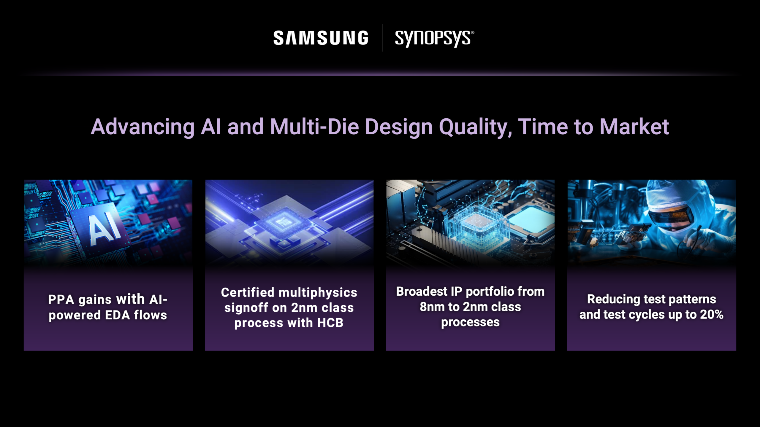
The central claim is that Synopsys.ai, a full-stack AI-driven EDA suite, is now certified for Samsung Foundry’s most advanced gate-all-around (GAA) processes. This is a critical step, as moving to 2nm is not just an incremental shrink but a fundamental shift in transistor architecture. For designers, this promises better power, performance, and area (PPA) — the holy trinity of chip design. However, the true test of the technology lies not in a press release, but in silicon yields.
The High-Stakes Battle for EDA Dominance
For decades, the EDA market has been a fiercely competitive oligopoly, and the advent of AI has only intensified this rivalry. The main contenders are Synopsys, Cadence Design Systems, and Siemens EDA. What sets them apart is built on decades of accumulated data, proprietary algorithms, and deep, symbiotic relationships with foundries like Samsung and TSMC. An EDA tool that isn’t certified by a leading foundry is practically useless for cutting-edge designs.
Sources close to the matter reveal that the real “AI” in this innovation is less about sentient machines designing chips and more about sophisticated machine learning models trained on immense datasets of previous chip layouts. These models can predict hotspots, optimize signal routing, and verify timing with a speed and accuracy that surpasses human capability. This is the technological high ground that Synopsys is defending with its latest announcement.
This move has not gone unanswered. Cadence, with its Cerebrus Intelligent Chip Explorer, and Siemens EDA are also heavily invested in AI-driven workflows. The critical differentiator often comes down to the quality and exclusivity of the training data provided by the foundry partner. This makes the tight integration between Synopsys and Samsung a potent barrier to entry, forcing competitors to forge equally strong alliances. The future of the system will likely be defined by these strategic partnerships.
You might also like: Power electronics: A Critical Warning for the Semiconductor Sector
A Critical Look at the Samsung-Synopsys Breakthrough
The most scrutinized part of the announcement is the term “production-ready” for 2nm processes. While Synopsys and Samsung have indeed certified a design flow, this is a far cry from mass production. Deeper analysis shows that the leap to 2nm and below involves solving immense physics and material science challenges that software alone cannot fix. High-NA EUV lithography, novel transistor structures, and new interconnect materials are all sources of potential yield-killing defects.
The announcement focuses on the ability of it to “accelerate design closure and optimize PPA,” which is a significant software achievement. The collaboration aims to shorten turnaround times for complex designs. Yet, it sidesteps the brutal reality of hardware manufacturing. Tech analysts at sites like AnandTech have consistently noted that node names like “2nm” are now more marketing metrics than precise physical measurements, making it difficult to compare processes between foundries.
Therefore, it’s more accurate to view this as a foundational step, not a finished solution. The the platform tools provide a powerful framework for designing at 2nm, but the actual manufacturability and economic viability of those designs are still open questions. Until Samsung demonstrates high-volume, high-yield production of 2nm chips designed with these tools, a healthy dose of skepticism is warranted. This is a prime example of software innovation moving faster than the underlying hardware can support.
The Black Box Problem and Regulatory Headwinds
As the technology becomes more integrated into chip design, a significant technological contradiction emerges. These AI systems are often “black boxes,” meaning even their creators cannot fully explain the reasoning behind every specific optimization. This creates a major challenge for verification and debugging. How do you guarantee a chip is free of flaws if the tool that designed it has an element of inscrutable logic?
This issue has not gone unnoticed by experts. A recent report from the Stanford Institute for Human-Centered Artificial Intelligence (HAI) highlighted the potential for AI-generated designs to contain hidden vulnerabilities or “trojans” that could be exploited. These flaws might be unintentional byproducts of the AI’s optimization process or, in a more sinister scenario, deliberately inserted. This risk is especially high in designs for critical infrastructure, defense, and autonomous systems.
This development is also catching the eye of governments and regulators. As a handful of companies and nations come to dominate the ecosystem for ai-powered eda, concerns about supply chain security and technological sovereignty are growing. We can expect to see more calls for transparency, auditability, and standardization in AI-based design tools. The era of EDA operating in a relatively unregulated space may be swiftly coming to an end.
Also read: Quantum technology: Critical Flaw Exposed in Quantum Tech Forecasts
The Bottom Line on ai-powered eda
To conclude, the Synopsys-Samsung partnership represents a major milestone for the semiconductor industry. It confirms that ai-powered eda is no longer a theoretical concept but a core component of designing the world’s most advanced chips. However, the claims of a seamless, production-ready 2nm flow should be viewed with significant skepticism. This is a powerful evolutionary step, but it is not the revolution that the marketing materials suggest. The path to true AI-driven chip manufacturing is fraught with physical, logical, and even geopolitical challenges.
Critical Signals to Watch:
- Monitor: The first public reports on actual 2nm wafer yields from Samsung using the new ai-powered eda toolchain.
- An important sign: A competitive response from Cadence or Siemens EDA announcing a similar level of integration with a major foundry like TSMC.
- Growing concern: Any new regulatory frameworks or export controls from the US, EU, or China targeting ai-powered eda technology.
- Technical benchmark: The publication of independent, peer-reviewed analysis comparing the PPA results of AI-designed chips versus human-optimized designs.
- Pay attention to: The adoption rate of these advanced tools beyond flagship customers for more mainstream chip design projects.
Ultimately, the trajectory of ai-powered eda is one of the most critical technology stories of 2026. Its success or failure will directly impact everything from artificial intelligence and supercomputing to the next generation of consumer devices.