
In a move shaking the foundations of AI infrastructure, Nvidia has unleashed a multi-billion dollar spending spree on the technology, a technology that transmits data using light. Since March 2026, the AI giant has plowed at least $6.5 billion into key developers like Lumentum and Coherent, betting that optics can solve the crippling energy and data bottlenecks threatening to stall progress. The official narrative, echoed by CEO Jensen Huang, is that the world needs substantially more this innovation capacity than currently exists to power the AI factories of the future.
Table of Contents
However, a deeper investigation raises serious questions. While the promise of breaking through the “Copper Wall” that limits traditional electrical interconnects is tantalizing, this massive capital injection looks less like a guaranteed revolution and more like a high-stakes attempt to brute-force a technology that is fraught with underlying challenges. Is the system the savior of AI, or is Nvidia simply buying up a supply chain fraught with hidden risks?
Mapping the Photonics Power Play
To grasp the present dynamics, one must look beyond Nvidia’s recent headlines. While Nvidia’s investments are monumental, the it landscape is a mature battlefield with entrenched players. For years, Intel has been a quiet giant in this space, having shipped millions of Photonic Integrated Circuits (PICs) since 2016 and leveraging its own fabs for vertical integration. The market is a complex web of strategic alliances, with Broadcom, Marvell, and Cisco also commanding significant territory. Nvidia’s strategy appears to be a direct assault to secure a supply chain it does not control.
The technical “moat” in the platform is formidable. The core challenge is not merely sending light down a fiber; it’s about the heterogeneous integration of multiple materials and components—lasers, modulators, detectors, and silicon waveguides—onto a single, compact, and reliable package. This process is famously challenging, facing issues with thermal management, material stress, and the microscopic precision required for packaging and alignment. These manufacturing and packaging complexities are the real bottleneck, a problem that throwing billions at component suppliers may not solve on its own.
Read also: Lima pump: The Breakthrough Facing a Critical Test
Deconstructing the AI Savior Narrative
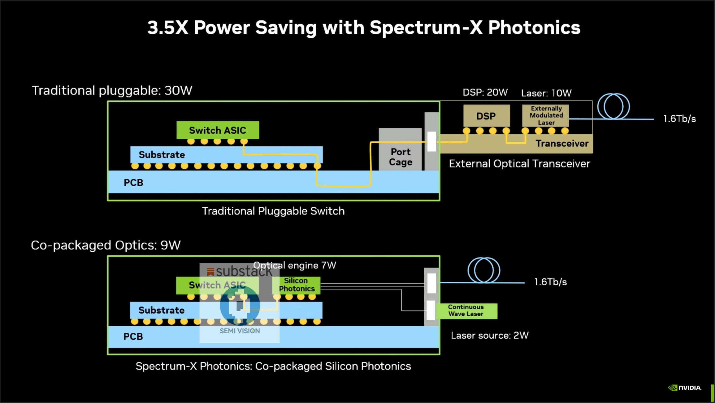
The primary narrative pushed by Nvidia is that the technology will solve the energy crisis in AI data centers. Photonics offers a way to scale This innovation without the debilitating energy costs of copper, which can consume nearly 30% of a cluster’s total power. Ayar Labs, a startup in which Nvidia has also invested, claims its optical I/O technology can deliver up to 20 times the computing throughput per watt compared to copper alternatives. This is the revolutionary promise driving the multi-billion-dollar investments.
But, a deeper analysis uncovers significant caveats. While the system is undoubtedly more energy-efficient per bit transferred, the manufacturing process itself presents a contradiction. The fabrication and, more critically, the packaging of these complex optical systems are incredibly intricate processes. As noted in a recent analysis from Laser Focus World, key challenges remain in energy efficiency at the system level, manufacturing scalability, and overall cost optimization. The risk is that while individual links are efficient, the total cost of ownership and the manufacturing yield rates could undermine the promised savings, an issue highlighted by market analysts at Yole Group who recently revised their market forecasts downward due to manufacturing yield concerns.
Uncovering the Core Friction Points
A core tension exists at the heart of the current it strategy. While the technology is pitched as the solution to AI’s scaling and power problems, its own path to mass production is riddled with challenges that could create new bottlenecks. Experts point to packaging, testing, and thermal management as the most significant hurdles to deploying ai infrastructure at the scale Nvidia envisions. The process of aligning lasers and fiber arrays to microscopic silicon waveguides with near-perfect precision is a major source of cost and potential failure, a far cry from the mature processes of traditional chip packaging.
This funnels control to a small number of specialized foundries and packaging houses, most notably TSMC, which is critical for the advanced 3D chip-stacking required for co-packaged optics (CPO). Any disruption at these facilities could halt global AI development. Furthermore, while Nvidia is locking up supply from key component makers, competitors like Intel are moving to offer silicon photonics manufacturing services to external customers, potentially creating a more open—and competitive—ecosystem. According to some analyses, the industry may be entering the “trough of disillusionment” for this technology, where early hype meets the harsh reality of implementation challenges. The true viability of ai infrastructure will be proven not in press releases, but in high-volume, cost-effective manufacturing.
Read also: Monolithic 3d integration: The Breakthrough That Could Reshape Computing
The Bottom Line on ai infrastructure
Ultimately, Nvidia’s $6.5 billion crusade is a forceful acknowledgment that the age of copper interconnects is over for high-end AI. The company is not just investing in a technology; it is attempting to vertically integrate the future physical layer of AI, mirroring its successful CUDA strategy. However, this is a considerably more dangerous bet. Unlike software, the physics of manufacturing and packaging ai infrastructure devices present unforgiving, real-world constraints. Nvidia is betting it can solve these deep engineering challenges through overwhelming financial force, but success is not at all assured.
Critical Signals to Watch:
- Keep an eye on: Manufacturing yield rates and the cost-per-port of co-packaged optics solutions. A failure to drive down costs could stall adoption.
- Key signal: Announcements from Intel’s foundry services regarding their silicon photonics offerings and customer traction.
- Next development: Breakthroughs in automated packaging and testing for photonic integrated circuits, which are currently a major bottleneck.
- Market shift: The emergence of competing optical interconnect standards backed by an AMD-led consortium, which could fragment the market.
- Geopolitical signal: Any disruptions at TSMC or other key advanced packaging providers, which hold the keys to manufacturing at scale.
The massive investment in ai infrastructure is now a central theater in the battle for AI dominance. Whether it becomes a revolutionary enabler or a monument to expensive hype will define the trajectory of computing for the next decade.