
In a development that is sending ripples across the technology sector, researchers at the University of Illinois Grainger College of Engineering have unveiled a new method for creating a true monolithic 3d integration. This isn’t just another incremental step; the team, led by professor Qing Cao, claims their low-temperature manufacturing process using ultra-thin silicon membranes finally overcomes the thermal budget constraints that have long plagued the technology. The promise is nothing short of extending Moore’s Law by building processing power vertically, like skyscrapers, instead of continuing the endless suburban sprawl of 2D chip design.
Table of Contents
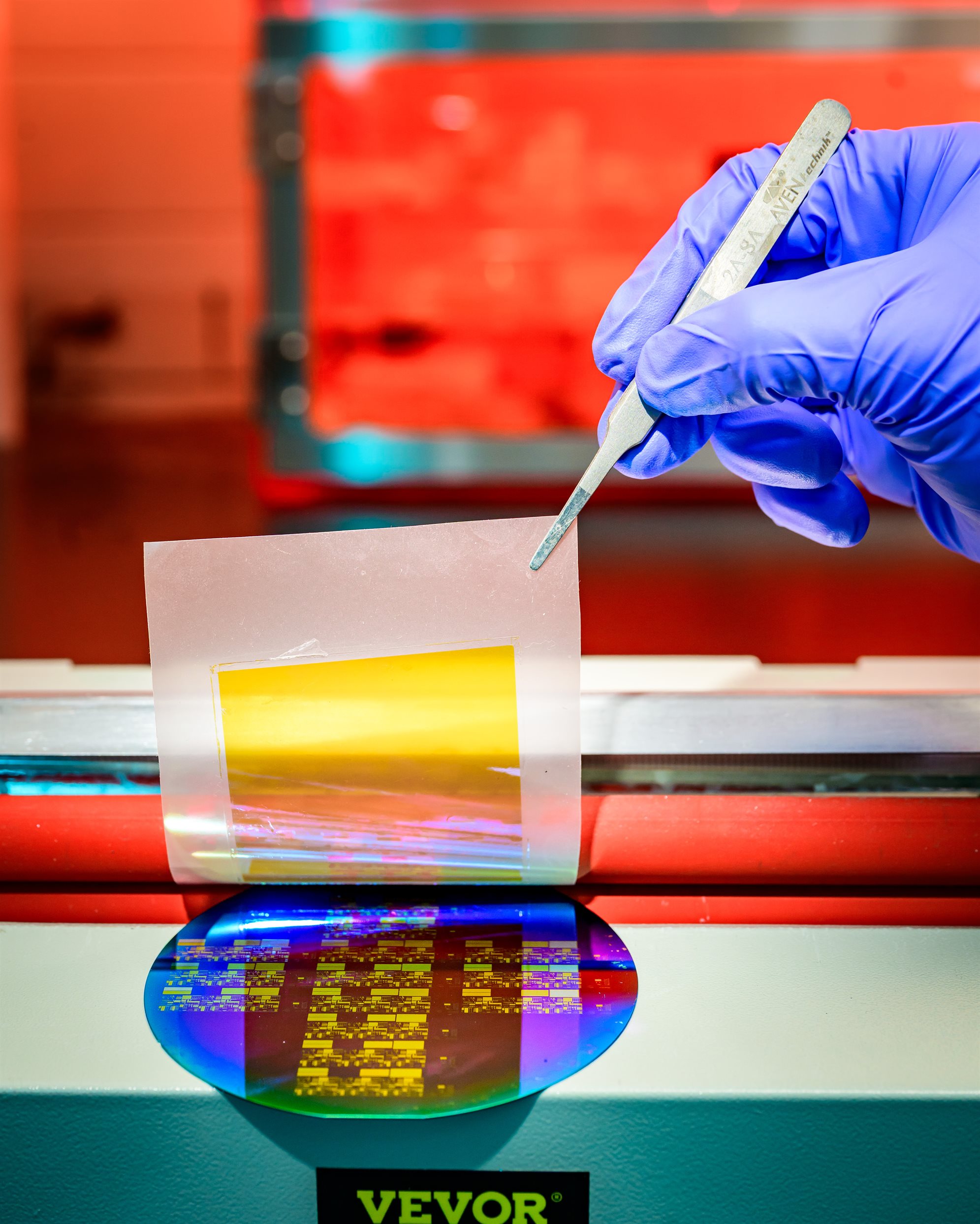
The core claim is that this technique enables the stacking of multiple layers of high-quality, single-crystalline silicon, the bedrock of modern electronics, with reported device yields of 98–100% in a lab setting. This development arrives at a critical juncture, as the industry grapples with the physical limits of miniaturization. But while the headlines herald a new era, seasoned analysts are asking the tough questions: can this academic success translate to the brutal, high-volume world of commercial fabrication?
Mapping the Competitive 3D Landscape
To grasp the significance, one must recognize that the concept of a this innovation is not entirely new. The industry has been pursuing vertical integration for years, primarily through “chiplet” or “2.5D” approaches. Leading players like Intel with its Foveros technology and TSMC with its System on Integrated Chips (SoIC) platform have already commercialized products that stack pre-fabricated dies. These methods connect separate, smaller chiplets with micro-bumps or through-silicon vias (TSVs), which, while effective, are fundamentally different from the “monolithic” ideal.
The existing approach is akin to building a multi-story building by stacking prefabricated modules. In contrast, the monolithic the system that the Illinois team is proposing is like constructing the entire skyscraper floor by floor, with wiring running natively between levels. This monolithic integration promises far denser and more efficient connections, potentially reducing latency and power consumption. However, the primary obstacle has always been heat. Fabricating a new layer of transistors typically requires temperatures so high they would destroy the circuits on the layer below. The Illinois breakthrough purports to solve this with a low-temperature process, a claim that, if scalable, could indeed be revolutionary.
Related article: Lima pump: The Breakthrough Facing a Critical Test
The established players in this space, TSMC and Intel, are not standing still. TSMC’s 3DFabric, which includes SoIC, CoWoS, and InFO, offers a comprehensive suite of advanced packaging solutions that allow customers to mix and match chiplets to optimize for performance and cost. Similarly, Intel’s Foveros Direct is moving toward solderless copper-to-copper hybrid bonding, pushing for sub-10 micron interconnect pitches to dramatically increase density. Any new it technology must compete with these deeply entrenched and continuously evolving ecosystems.
Illinois’s Claims vs. High-Volume Manufacturing Reality
Although the academic achievement is undeniable, transitioning from lab-scale success to mass production presents immense challenges. The claim of a low-temperature process that preserves the integrity of underlying layers is the linchpin of this entire breakthrough. Skeptical analysts will point out that thermal budget is just one of many obstacles.
A primary concern is yield and defectivity at scale. Achieving a 98% yield on a small number of devices in a lab is one thing; maintaining that across millions of chips on 300mm wafers is another challenge entirely. The platform multiplies the potential for defects, as a single flaw on any layer could render the entire stack useless. This complexity dramatically increases fabrication costs and requires unprecedented levels of process control.
Furthermore, the issue of routing congestion and thermal management does not simply disappear. While a monolithic the technology can shorten communication paths, the sheer density of transistors stacked so closely together can create intense thermal hotspots that are difficult to cool, potentially throttling performance and affecting reliability. The research acknowledges strong inter-tier thermal coupling, an issue that requires sophisticated thermal-aware design methodologies to mitigate. The industry will be watching closely for follow-up data on long-term reliability and performance under real-world thermal loads.
The Economic Contradiction: Performance Gains vs. Soaring Costs
The bottom line for this technology is whether it makes financial sense. The semiconductor industry is driven by the cost-per-transistor. While monolithic 3D stacking promises more transistors in a smaller footprint, the complexity of the manufacturing process could make it prohibitively expensive. Industry assessments suggest that high costs and fabrication complexity are primary factors restraining the growth of the monolithic 3D IC market.
Industry leaders are already making strategic bets on chiplet-based heterogeneous integration for this very reason. By using different process nodes for different chiplets (e.g., a cutting-edge node for CPU cores and a cheaper, older node for I/O), they can optimize costs in a way that a monolithic this innovation might not allow. The Illinois approach would need to demonstrate a clear and substantial performance-per-dollar advantage to convince foundries to re-tool their multi-billion dollar fabrication plants.
Also read: Meta ai pendant: A Critical Warning for Early Adopters
In addition to cost, the broader ecosystem presents hurdles. A shift to monolithic 3D design requires a complete overhaul of Electronic Design Automation (EDA) tools and established design workflows. A successful pivot requires a coordinated effort across the entire industry. The University of Illinois team notes its work was supported by industry partners including IBM, Intel, and TSMC, which is a positive sign for future technology transfer, but the road from partnership to mass adoption is long.
The Bottom Line on monolithic 3d integration
To sum up, the Illinois breakthrough represents a crucial scientific advance in the quest for a monolithic the system. It directly addresses the critical thermal budget problem that has long been a primary blocker for it. However, it is not a silver bullet. The leap from a lab-proven concept to a commercially viable, mass-produced product is immense, with substantial hurdles in yield, cost, thermal management, and ecosystem development still ahead. This is less of a finished revolution and more of a critical battle won in a long and arduous war to redefine the future of computing.
Critical Signals to Watch:
* Monitor: Any announcements of a pilot production line or technology transfer to a major foundry like TSMC or Intel.
* Key signal: Publication of independent data on large-scale wafer yield and defect density for this process.
* Key signal: Competing low-temperature monolithic process announcements from industrial R&D labs.
* Key signal: The emergence of new EDA tools specifically designed for monolithic 3D architectural planning and thermal analysis.
* Key signal: An independent cost-per-transistor analysis comparing this new monolithic 3d integration approach to advanced chiplet packaging like Foveros Direct and SoIC.
Currently, this is best understood as a foundational research breakthrough that could reshape the industry in the coming decade. The development of a scalable monolithic 3d integration remains one of the most important frontiers in technology, and while the path is challenging, this work from Illinois has illuminated a promising way forward.