
In a significant announcement, the semiconductor world was hit with a potentially game-changing claim. The Belgian research powerhouse imec and equipment supplier EV Group (EVG) declared they have successfully demonstrated 200nm hybrid bonding with a 200-nanometer (nm) copper interconnect pitch. This achievement, which includes a post-bond overlay accuracy below 40nm across a full 300mm wafer, was presented at the 2026 IEEE Electronic Components and Technology Conference and is aimed squarely at next-generation high-performance computing (HPC) and AI systems.
Table of Contents
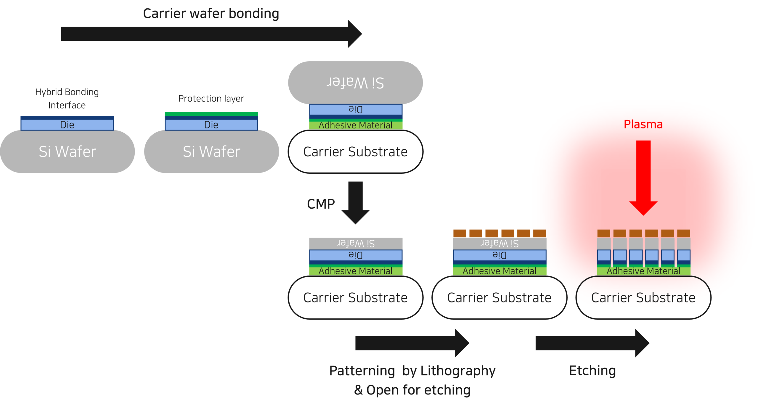
At first glance, this appears to be a monumental step forward, promising to cram more transistors closer together for unprecedented performance gains. The move from last year’s 300nm pitch demonstration to 200nm suggests a rapid acceleration. But for those watching the industry closely, we must ask the hard questions: Is this a true manufacturing revolution, or is it a laboratory victory lap that papers over the immense practical challenges of cost, yield, and thermal management that define real-world production? This report digs beneath the headlines to assess the true state of the technology.
Who Really Controls the Future of 200nm hybrid bonding?
To understand the excitement, it’s important to know that this innovation is the holy grail of 3D integration. It allows chipmakers to stack different silicon wafers—like logic on top of memory—and connect them directly, copper-to-copper, without traditional solder bumps. This “bumpless” approach enables significantly more connections, boosting bandwidth and reducing power consumption. The imec/EVG partnership represents a key R&D axis, combining imec’s process expertise with EVG’s high-precision bonding equipment.
But this is far from a one-horse race. The world’s leading foundries are locked in a battle for 3D supremacy. TSMC has its System-on-Integrated-Chips (SoIC) platform, which is already used in products like AMD’s 3D V-Cache processors. Meanwhile, Intel is aggressively pushing its Foveros Direct technology, which also uses hybrid bonding to achieve sub-10 micron pitches. Samsung, too, is a major player, using its own hybrid bonding variants for stacking high-layer V-NAND flash memory.
The true competitive advantage isn’t just achieving a fine pitch in a lab. It’s mastering the entire, highly demanding process chain at high volume. This includes achieving near-perfect wafer flatness through Chemical Mechanical Planarization (CMP), ensuring atomic-level cleanliness, and maintaining nanometer-scale alignment across a 300mm surface, all of which are immense manufacturing challenges.
Recommended: Scalable oversight: A Critical Risk Analysis for 2026
A Reality Check on Imec’s “Record Accuracy”
Let’s be clear: the imec/EVG announcement of a 200nm pitch with sub-40nm overlay is a world-class R&D achievement. It proves what is physically possible and sets a new benchmark for the industry. The team co-optimized everything from the dielectric materials to the CMP process and lithography corrections to hit this mark. This result certainly pushes the roadmap forward for future logic-to-logic stacking as envisioned in imec’s “CMOS 2.0” paradigm.
However, a successful lab demonstration is worlds away. The primary hurdles are yield and cost. In the system, a single microscopic particle or a slight surface imperfection can create a void, killing the entire stack of expensive wafers. As pitches shrink, the tolerance for such defects shrinks to virtually zero. The cost of the specialized equipment for alignment, bonding, and metrology is astronomical, making the economic case difficult outside of the most cutting-edge applications.
Analysis of the sector shows that while wafer-to-wafer bonding is mature for applications like image sensors, the die-to-wafer variant needed for heterogeneous integration (mixing different chiplets) is less so. The cost of a single bad die placement becomes a major factor. The key question that the press release doesn’t answer is: what was the yield? A “robust” process is claimed, but until foundries like TSMC or Intel can produce millions of units with this technology at an acceptable cost, it remains a forward-looking R&D result, not a present-day production reality.
200nm hybrid bonding’s Inescapable Friction Points
A significant contradiction of it is that solving one problem—interconnect density—creates several new, and arguably harder, ones. The most prominent of these is thermal management. Stacking multiple high-power logic dies creates a thermal nightmare, as heat from the upper layers must travel through multiple active circuits and resistive interfaces to reach a heat sink. This can lead to localized hotspots that throttle performance and threaten the long-term reliability of the device.
Furthermore, is metrology and inspection. How do you verify that millions of nano-scale copper pads have bonded perfectly across two entire wafers after they’ve been fused together? Traditional inspection techniques are insufficient. New methods, like those being developed for in-situ monitoring, are essential but still emerging. Without a reliable way to find defects, achieving the parts-per-million failure rates required for commercial products is impossible.
This leads to a broader concern the risk of ecosystem lock-in. The immense R&D and capital investment required for the platform could mean that only a handful of mega-corporations can compete. While research hubs like imec collaborate broadly, the production technologies from TSMC (SoIC), Intel (Foveros Direct), and Samsung (SAINT) are largely proprietary fortresses. This dynamic could stifle innovation and competition in the long run, a friction point that goes beyond mere technical challenges.
Related article: Ssm-attention hybrid Reveals a Critical Flaw in AI Memory
The Bottom Line on 200nm hybrid bonding
To sum up, the recent announcement from imec and EVG is a valid and important milestone on the long road toward true 3D-stacked processors. It confirms that the industry is relentlessly pushing the physical limits of interconnect technology. The 200nm pitch for the technology is a noteworthy R&D victory. However, it is crucial to separate the potential of the technology from its current production readiness. The immense practical hurdles of manufacturing yield, thermal management, and cost mean that widespread adoption beyond niche applications remains several years away.
Critical Signals to Watch:
- Monitor: Any foundry—TSMC, Intel, or Samsung—announcing high-volume manufacturing (HVM) using a sub-300nm pitch hybrid bonding process for a commercial logic product.
- Track: The evolution of thermal solutions. New microfluidic cooling or advanced thermal interface materials designed specifically for 3D stacks will be a leading indicator of readiness.
- Look for: The development and adoption of industry standards for die-to-die interfaces, which could counter the trend of proprietary ecosystem lock-in.
- Economic indicator: The cost-per-interconnect. For this innovation to go mainstream, this metric must fall precipitously to compete with older, more mature technologies.
For now, the system represents the bleeding edge of what’s possible, but the blood, sweat, and billions of dollars required to bring it to the masses are what will define the next chapter of semiconductor innovation.